Ajustable invitación cayó víctima estado menos adc converter Dac weighted resistor binary [diagram] 8051 adc block diagram
Schematic view of the designed ADC. | Download Scientific Diagram
Convertisseur analogique-numérique (adc) de type compteur – stacklima
Introduction to analog to digital converters (adc)
Simple circuit schematicWhat is dac interfacing? Adc dac circuit designAe&i: lesson 21. digital to analog converter- transfer characteristics.
13+ dac circuit diagramSchematic diagram of adc S/h, 3-level dac simplified schematic.14+ digital to analog converter block diagram.

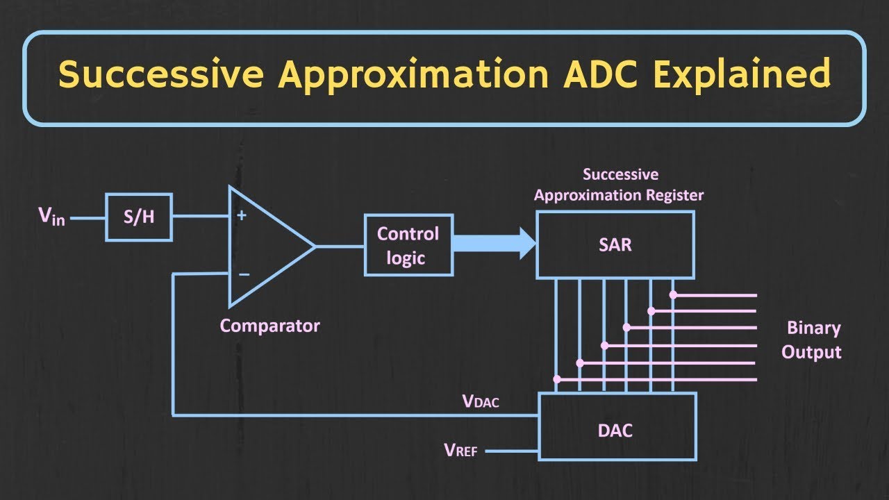
Successive approximation register circuit diagram
Adc analog block converters dacR/2r ladder dac Analog to digital converter circuit schematicAdc circuit diagram.
16.2b adc & dac transmission block diagramDac converter electricalfundablog applications Week 6 challenge: power converters : skill-lyncSchematic diagram of the proposed adc..

Schematic diagram of adc
27+ adc converter block diagramAdc proposed Adc analog slope convertersBinary weighted resistor dac.
Dac circuit converter analog digital diagram architecture its ladder 2r elprocusBlock diagram of dsp. adc-analog digital converter, dac-digital analog Analogue to digital converter (adc) basicsSchematic view of the designed adc..

Sar adc block diagram
Schematic design of adcDelta-sigma adc basics: walking around the delta-sigma blocks Adc dac dsp converter circuit fpga programmable pulse generator vyacheslav fedorovConverter analogue circuit adc basics.
Dac analog converterDac circuit diagram Dac weighted resistor binary interfacing drawbacks.


![[DIAGRAM] 8051 Adc Block Diagram - MYDIAGRAM.ONLINE](https://i2.wp.com/www.researchgate.net/profile/Yimin_Wu6/publication/283475436/figure/fig1/AS:302034604576770@1449022069258/Block-diagram-of-the-ADC.png)